On-Chip LLM: War Stories and the Method
Bit-honest before fast. Where iverilog lies, why silicon beats the timing report, and the optimisation that won and got stopped anyway.
Part of the on-chip LLM on a $250 FPGA series. The discipline that made the numbers trustworthy, and the scars.
The rule is: bit-honest before fast. Every block is proven bit-exact (or cosine > 0.9999 for the transcendental approximations) against a Python reference before anyone runs a synthesis: The compile step that turns RTL into a netlist of actual gates and FPGA primitives, before place-and-route. or quotes a speed. The toolchain is hand and LLM written RTL: Register-Transfer Level: the abstraction (and the SystemVerilog/Verilog code) used to describe the actual digital circuits. (there is no HLS: High-Level Synthesis: tools that compile C/C++ into hardware so you don't write Verilog by hand. This project has none; every block is RTL written directly, by me and by Claude Code, never compiled from C. on the build box), gated in iverilog: Icarus Verilog: the open-source simulator used for the fast local correctness loop before the slow Vivado build. simulation, then implemented in Vivado: Xilinx's FPGA design suite: synthesis, place, route, and bitstream generation., then verified on the board with three matching runs.
Some scars from the road, because they are the actual content of the work:
- Simulation lies in specific, learnable ways. iverilog silently ignores out-of-range array reads and returns X, while real silicon wraps the address. One such bug, once found, made the design 14,336 cycles per token faster. Asynchronous reads pass every simulation gate and then do not exist on real BRAM: Block RAM: small, flexible on-chip SRAM blocks (~5 Mb total). Holds activations, scratch, and the KV cache here.. The fix is to never trust a gate you have not also run on the metal.
- Silicon is faster than the timing report says. Static timing: Static Timing Analysis: the tool's conservative estimate of the fastest clock a design can run at. On this part it is pessimistic by 1.3x to 1.76x versus real silicon. on this part is pessimistic by 1.3x to 1.76x. Designs that close at 70 to 85 MHz on paper run bit-exact at 125 to 200 MHz on the board. So the policy is: build at a clock that closes, then find the real ceiling with a board-side frequency sweep, and never quote the number until the tokens match.
- Build outside OneDrive. The repo lives in a OneDrive folder, and OneDrive’s cloud-sync filter will lock multi-gigabyte build files mid-run and corrupt them. Every build scratch dir lives on a plain local path. This cost a confusing afternoon exactly once.
- The race I won and stopped anyway. There was a whole campaign (“the double-pump”) to run the multiplier at twice the fabric clock. It worked, it was bit-exact on silicon, and it could not beat the record on this chip, all three at once, because a faster clock island still has to be fed by the fabric, and the fabric was the wall the whole time. The correct engineering move was to write the post-mortem and stop, rather than chase a beat-by-a-nose past a wall we had already documented. Knowing when to stop is a result too.
The ladder
Every green rung is measured on silicon, three runs, token stream bit-exact against the integer reference.
fabric/progress.py plus the live bench, 28 rungs. Tap or click a rung for what that step removed. Acts I to III count aggregate tokens across parallel streams; Act IV is the faithful single-stream metric with full context, ending at the live operating record of ~21,300 tok/s, held flat from 1 to 2,000 concurrent connections (peak 21,479, zero errors; counted-cycle record 19,242 at 200 MHz).| Step | tok/s | The idea |
|---|---|---|
| A53 char chat | 11 | the CPU baseline, the wall |
| HW sequencer @40 MHz | 44 | take the CPU out of the loop entirely |
| wide P-lane datapath | 1,883 | one URAM word feeds 128+ lanes the same weight |
| N=8 single-pass | 19,276 | one weight pass serves 8 streams at once |
| N=16 + softmax cut | 25,744 | the stream ceiling (single weight pass) |
| split-brain N=14 | 36,971 | two 7-stream cohorts on the dual-port URAM |
| N=16 split-brain @ 200 MHz, full wave | 59,965.5 | the record (two cohorts of 8) |
Where it loses
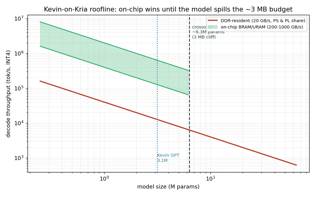
- The crossover. The on-chip trick wins only while the model fits on-chip. The roofline: The analytical plot of achievable throughput versus model size, showing where the on-chip advantage gives way to the DDR wall. says the crossover is around 6.3M parameters, roughly 3 MB of INT4: 4-bit integers (16 levels). The weights are stored as INT4, which is what makes the model small enough to fit on-chip.. Past that the model spills to DDR: The off-chip DRAM (the board's main memory), ~20 GB/s, shared by both the CPU and the fabric. This shared controller is 'the bandwidth wall'. and the fabric advantage evaporates back to the bandwidth wall. This is a toy-model technique by construction.
- The KV cache spills too. Long context blows the on-chip budget just like big weights do. The faithful build remembers a couple of short turns, not a document.
- 100k was a fantasy. The project chased a “100k tok/s” headline and then, honestly, disowned it: the real cycle floor on this architecture lands the ceiling around 62k to 78k on this chip, not 100k. The record is 59,965, and that is the number that gets quoted.
Back to the main post. The code is on GitHub.